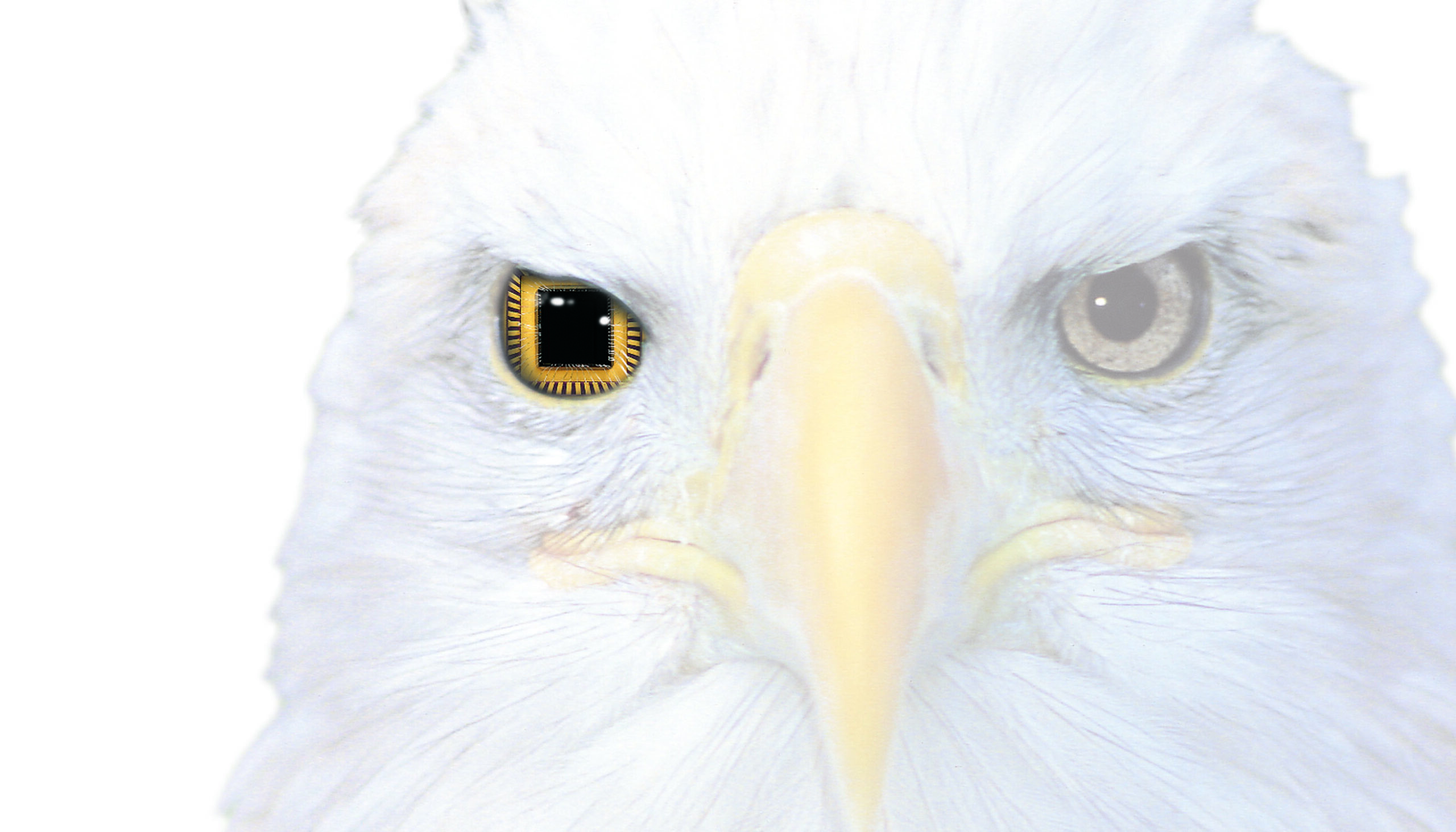
Latest Offering Designed for High-Resolution, Digital Still Camera Applications
SUNNYVALE, Calif. — April 23, 2001 — OMNIVISION Technologies, Inc. (Nasdaq: OVTI), a leader in designing, developing and marketing advanced, highly integrated CMOS image sensors used in electronic cameras and other optical imaging devices, today announced its new 1.3 mega-pixel (1280 x 1024) image sensors, designed for the digital still camera market where high-resolution output is required. The newest products are the latest in OMNIVISION’s portfolio of image sensors at many resolution levels; OMNIVISION additionally offers image sensor solutions for CIF (320 x 240), VGA (640 x 480) and SVGA (800 x 600) resolutions. The introduction of these mega-pixel products is the latest milestone for OMNIVISION in its commitment to provide high quality, high resolution image sensors to the digital still camera market.
“Reaching mega-pixel resolution is a major achievement for OMNIVISION,” said Bob Stroh, vice president of strategic marketing and business development. “Our strategy has been to provide outstanding products starting with the lower resolution level and working our way up to higher resolution levels. This strategy has served us well, and we now offer customers numerous high-quality CMOS products that scale from CIF to mega-pixel.”
The new mega-pixel products include the color OV9610 and black-and-white OV9110. These products, like many of OMNIVISION’s offerings, are targeted at the digital still camera market. For digital still cameras, 1.3 mega-pixels is generally considered the level of resolution required to print an image in a standard photo size. More pixels enable clearer printed images. While OMNIVISION’s CIF, VGA and SVGA products provide high-quality displayed images or smaller printed images, the mega-pixel products enable such applications as standard-sized printed photos and a wide range of other applications in security and machine imaging where more detailed images are desired.
More On The OV9610/9110
The OV9610 and OV9110 have a resolution of 1280 x 1024, with total pixels numbering 1312 x 1036. The sensor array is designed to work with a half inch lens format and is packaged in a 64‑pin LCC package. The sensors have square pixels with a 5.2 µm x 5.2 µm pixel pitch. The products have a true optical black and operate with a 24 MHz crystal with an internal phase locked loop (PLL). The 3.3 volt power supply enables low power consumption. Maximum frame rate of full array raw data readout is 30 frames per second. Maximum frame rate of YUV output, after color processing, is 30 frames per second. There are two channels of digital output, and the maximum data rate is 48 MHz. Selectable sub-sampling allows output of VGA (640 x 480) or CIF (320 x 240) resolution and both sensors support single frame output. The mega-pixel image sensors are highly integrated using the same proprietary technology used in OMNIVISION’s other CMOS image sensors which means that most image processing functions are integrated into the same chip as the image sensor array, including such functions as color processing, smart automatic or manual white balancing (AWB), fast automatic or manual exposure control, fast automatic or manual gain control and edge enhancement.
Pricing and Availability
In OEM quantities the color OV9610 is priced at $23.00 and the black & white OV9110 is priced at $21.50. Both image sensors are immediately available for sampling to qualified OEMs.
About OMNIVISION
OMNIVISION Technologies, Inc. designs, develops and markets high-performance, high-quality and cost-efficient camera chips. The company’s highly integrated image sensors are used in a variety of electronic cameras and optical imaging products for both still picture and live video applications. OMNIVISION provides all the functionality of a complete camera, and only a lens need be added. OMNIVISION is able to integrate many image system functions into a single chip instead of multiple chips required to achieve the same functions by competitive image sensors. The highly integrated design enables customers to design cameras that are lower in cost, smaller, lighter in weight, consume less power, are more reliable and more easily integrated with other circuits than cameras using multiple-chip image sensors. OMNIVISION is based in Sunnyvale, California. For more information about the company, visit www.ovt.com.
Certain statements in this press release, including statements regarding applications enabled by mega-pixel products are forward-looking statements that are subject to risks and uncertainties. These risks and uncertainties, which could cause the forward-looking statements and the company’s results to differ materially, include, without limitation: potential latent defects in the company’s products; the change of industry or consumer standards regarding accepted resolution levels for mega-pixel enabled applications and the other risks detailed from time to time in the company’s Securities and Exchange Commission filings and reports, including, but not limited to, the company’s quarterly reports filed on January 31, 2001. The company disclaims any obligation to update information contained in any forward-looking statement.
