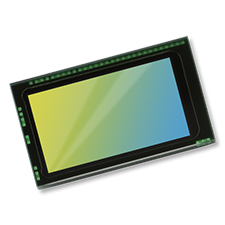
OmniBSI™-2 Technology
OMNIVISION’s OmniBSI™-2 technology extends OmniBSI™ to enhance the signal level in image sensors
Technology Benefits
OmniBSI™-2 image sensors reduce power consumption and enable more advanced image quality than OmniBSI™.


Technology Features
OmniBSI™-2 features advanced process node design rules and 300mm wafer process to enhance camera performance and capabilities.
-
65nm Design Rules65nm design rules enable compact pixel circuitry for optimal pixel layout to maximize performance for enhanced image quality.
-
300mm Wafer Process300mm wafer process improves the stability of production and increases die per wafer for high-volume production applications.
-
Backside Illumination (BSI)Backside illumination flips pixels and circuitry to collect the light from the backside of the image sensor.
Applications
OMNIVISION’s OmniBSI™-2 targets mobile, security, medical, automotive and notebook/PC applications.
Product Solutions
OMNIVISION places its customers at the leading edge of imaging technology with its commitment to innovative, forward-thinking solutions.
What’s New
Stay up to date with all of OMNIVISION’s news, announcements and updates.


